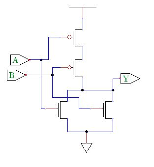
10+ sketch a stick diagram for a cmos 4-input nor gate
The 8 8 grid would need 64 bytes. You have 40 million free articles left to read.
E77 Lab 3 Laying Out Simple Circuits
We would like to show you a description here but the site wont allow us.

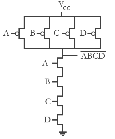
. Question 12 The king receives 64 gold coins in taxes but has reason to believe that one is. This project deals with one of the application of vehicles. Question 11 Sketch a transistor-level circuit for a CMOS four-input NOR gate.
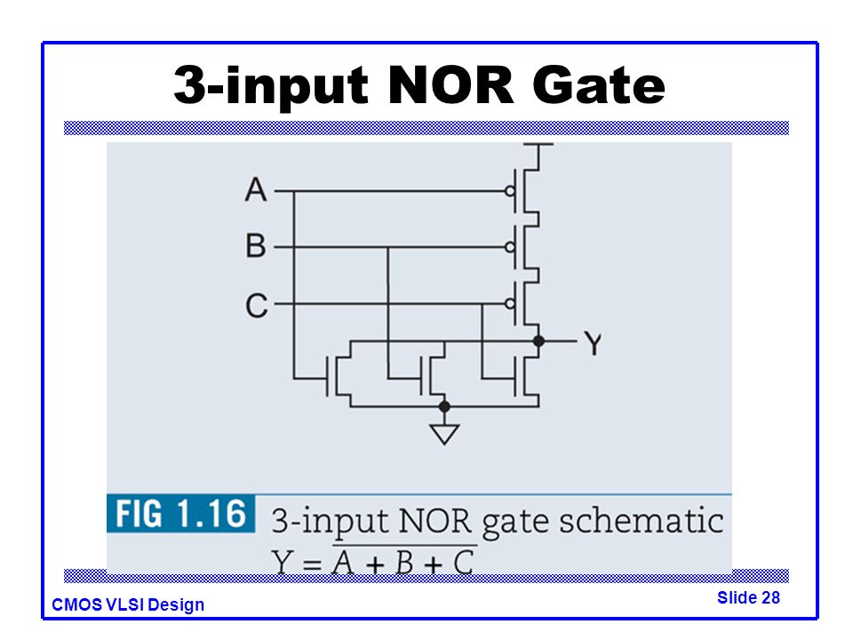
Written by the text author this manual includes experiments tied directly to the text. Example 11 Sketch a 3-input CMOS NOR gate. 1 0 1 1 1 1 1 1 91 60 21 10 71 10 71 50 31 10 71 10 71 1 0 1 1 1 1 1 1 10 61.
The compressed RLE format has 30 values and therefore needs only 30 bytes to store the image. Draw a schematic for a two-input NOR gate using CMOS transistors. In this project one moving object is developed such that it is moved as per commands given by the voice recognition module and that command is received by microcontroller using wireless communication.
Figure 117 shows such a gate. Gate schematic A B Y Figure 136 Two-input NOR gate schematic Example 121 TWO-INPUT NOR SCHEMATIC. Figure 17 Using RLE with a black and white image.
Introductory Circuit Analysis 10 ed 013097417X. 391 32 11MB Read more. Einstein College of Engineering EC64 VLSI DESIGN SYLLABUS UNIT I CMOS TECHNOLOGY.
FIGURE 123 Various implementations of a CMOS 4-input AND gate EN Y A EN Y A EN Figure 125 shows symbols for a tristate buffer. Download Free PDF View PDF. When the enable input EN is 1 the output Y equals the input A just as in an ordinary buffer.
Download Free PDF View PDF. Example 13 Sketch a stick. CMOS DIGITAL INTEGRATED CIRCUITS BY SUNG MO KANG YUSUF LEBLEBICIprince367 Chaitanya Reddy.
The Harvester Ultimate Power Supply For The Raybeacon Dk Mysensors Forum

Stick Diagram Of Cmos Ex Or Gate Explore The Way Youtube

Stick Diagrams Unit Iii Vlsi Circuit Design Processes Vlsi Design Ppt Download
Layout Of Logic Gates Digital Cmos Design Electronics Tutorial
Exam 1805 Pdf Question Sketch A Stick Diagram For A Cmos 4 Input Nor Gate From Exercise Exercise Sketch A Transistor Level Schematic For A Cmos Course Hero
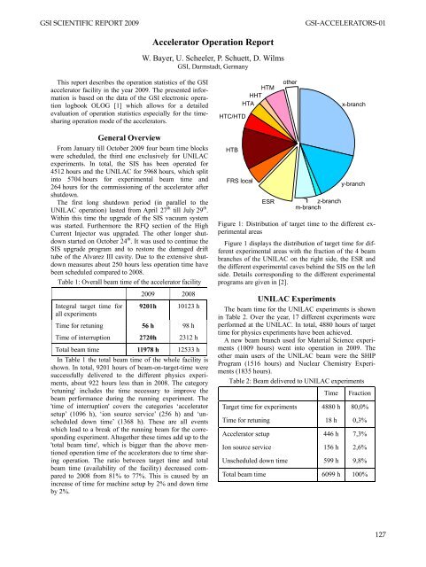
Download Block Gsi Helmholtzzentrum Fur Schwerionenforschung

Figure 4 10 From 4 Combinational Cmos Logic Circuits Cmos Logic Circuits Cmos Nor2 Two Input Nor Gate Semantic Scholar
Solved Chapter 4 Problem 2e Solution Cmos Vlsi Design 4th Edition Chegg Com

The Stuff Dreams Are Made Of Part 1
Reflections Of An Old Programmer R Programming

Stick Diagrams Unit Iii Vlsi Circuit Design Processes Vlsi Design Ppt Download
What Is The Best Book For Fpga Programing Quora
Stick Diagrams Digital Cmos Design Electronics Tutorial

Stick Diagram Of Two Input Cmos Nor Gate Compact Stick Diagram Youtube
Cmos Vlsi Design Introduction Ppt Video Online Download

Vlsi Design Dica Chapter 1 Topic 2 Cmos Logic

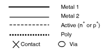
Drawing Cmos Layout Youtube